
HDI PCB Manufactured
High-density interconnect (HDI) printed circuit boards offer improved performance, reliability and design freedom for electronic devices. They feature thinner traces, smaller vias and more layers. They also provide a faster signal transmission speed and better power management. They are often used in complex devices like cell phones, digital cameras and 4G network communications, as well as military applications, such as avionics and smart munitions.
A HDI PCB’s manufacturing process differs from traditional PCBs in a few ways. It includes multiple lamination cycles and sequenced stacks. In this process, copper and pre-preg layers are combined with each other by applying heat and pressure to the PCB. Afterward, the layers are assembled to create a multi-layer board. During this process, the fabricator needs to maintain strict layer registration. Failure to do so can result in one-side warpage, which dramatically decreases the yield of the board. Moreover, the fabricator must ensure that the drilled vias are aligned with the correct layer on each side of the PCB.
The central feature of a hdi pcb is the microvias, which have to be designed precisely to accommodate routing between layers. This helps reduce manual routing work and offers a wider space for component placement. It also enables the use of lower aspect ratios, which allows for more components in a smaller area. This increases the performance and reliability of the board and allows it to function in harsh environments.
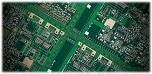
How is an HDI PCB Manufactured?
In addition, the use of microvias can lower the overall costs of a HDI PCB. This is mainly because it requires less copper and eliminates the need for through holes. In turn, this lowers the cost of the materials and the production time required to assemble a PCB. Moreover, the use of microvias can help reduce the number of manual steps and error rates during assembly.
Additionally, the high-speed signal transmission capabilities of HDI PCBs have made them popular for use in consumer electronics such as smart watches and mobile phones. In addition, they are increasingly being used in medical devices. In fact, some advanced electronic medical devices that perform monitoring, imaging, surgical procedures and laboratory analysis have been engineered with HDI technology.
In addition, HDI PCBs can be found in industrial equipment such as warehousing and inventory control systems. These devices can monitor machinery performance and relay information to management and employees. In turn, this can improve productivity and reduce maintenance costs. These uses have helped to promote the adoption of HDI PCBs in industrial settings. As a result, this has shaped the future of industrial technology and helped to drive new innovations. In order to meet these new demands, manufacturers have implemented rigorous quality control procedures that uphold precision and reliability. This is achieved by utilizing advanced inspection technologies and ensuring adherence to industry standards and certifications. Ultimately, this allows manufacturers to produce exceptional and reliable HDI PCBs that meet consumer requirements and industry standards.